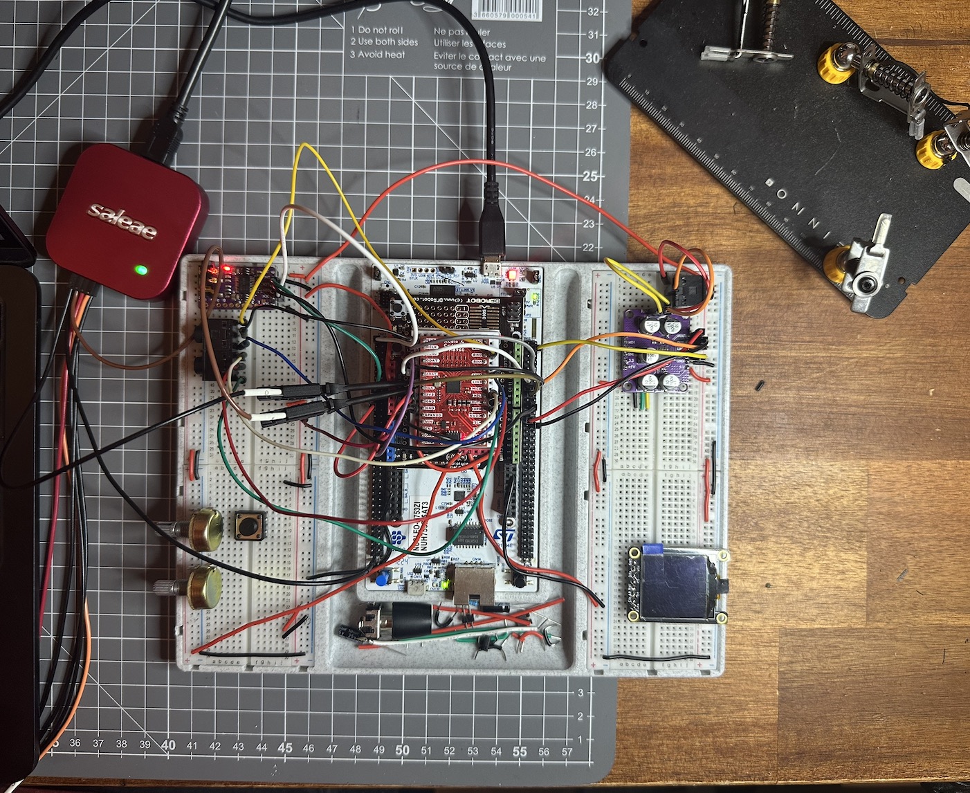
I’ve recently embarked on a journey to create a digital effects unit (like a guitar pedal, but not a guitar pedal).
It’s been incredibly interesting so far, learning a lot about various
different topics, which is as frustrating as it’s rewarding (ok, maybe a bit more
rewarding).
What I present here may seem straightforward for some, but it was quite a
laborous endeavour packed with trial and error and scarce online resources.
This post aims to share some knowledge about what I’ve learned, for my future self and for anyone else struggling with this too!
The bird’s eye view is this:
                                ┌────────────┐┌────────────┐
                                │  Jack In   ││  Jack Out  │
                                └────────────┘└────────────┘
                                    │             ▲
                                    │             │
                               ┌────┘             └────┐
                               │  ┌─────────────────┐  │
                               └─▶│      CODEC      │──┘
                                  └─────────────────┘
                                           ▲
                                           │
                                           ▼
                                   ┌─────────────────┐
                                   │       MCU       │
                                   └─────────────────┘
MCU selection
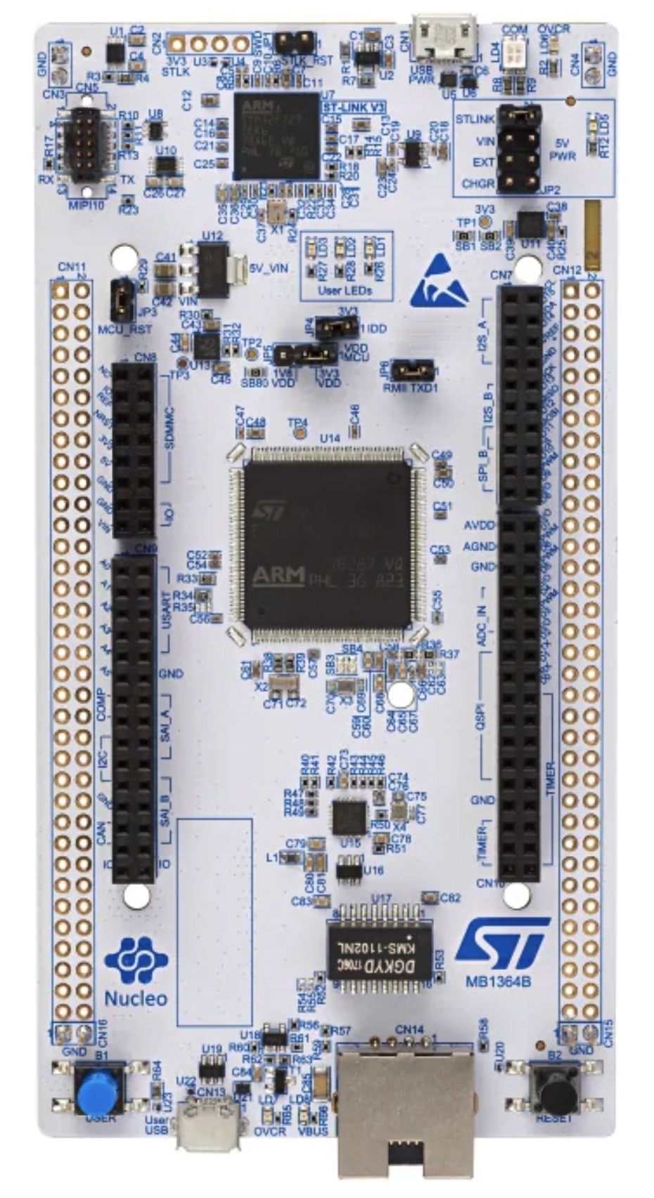
Since this project aims to be a real-time audio effects unit, we need something with good speed (to run the effects algorithms, plural) and decent RAM (some algorithms may operate over a group of samples), I decided to go with the STM32H753ZI.
Keys specs being:
- 480MHz
- Double Precision Floating Point Unit (FPU)
- 2MB Flash / 1MB RAM
- An LQFP package (easier to solder than QFN or BGA)
This is maybe overkill for my needs, this is something I can downsize down the line.
And another big deciding factor is that STMicroelectronics provides a devkit for this chip, with the Nucleo-H753 which is incredibly useful to start prototyping without worrying about the MCU circuitry (which will come at a later stage).
The Nucleo dev-boards also come with a builtin STLink which is used for flashing the chip and debugging.
STMicroelectronics provides a nice (and free) all-in-one IDE to work and debug their chips, CubeIDE.
The following assumes you are somewhat familiar with the setup of a basic
project, if not Digikey as a great video series
on the this topic.
CODEC chip selection
ADC primer
My requirements for the ADC/DAC is 24 of bit depth and 48KHz sampling rate minimum.
24 bits means that the resolution of the ADC for example is represented as a
signed integer (so from -2^23 to +2^23, the most significant bit being used
for the sign); sampling an analog
signal (continous by nature) to discrete values.
The bigger the range of values used to represent this continuous signal, the
higher the fidelity.
An extreme example would be a 2 bit ADC (from -1 to +1), where you would only be
able to represent “sound” and “no sound”.
And 48KHz is the frequency at which we’re sampling those 24 bits, see the wikipedia article on the Nyquist–Shannon sampling theorem for more information (44.1 is just a weird number…).
If you wish to dive deeper into this topic, xiph.org’s has a great video series going into details I never could.
Sparkfun <3
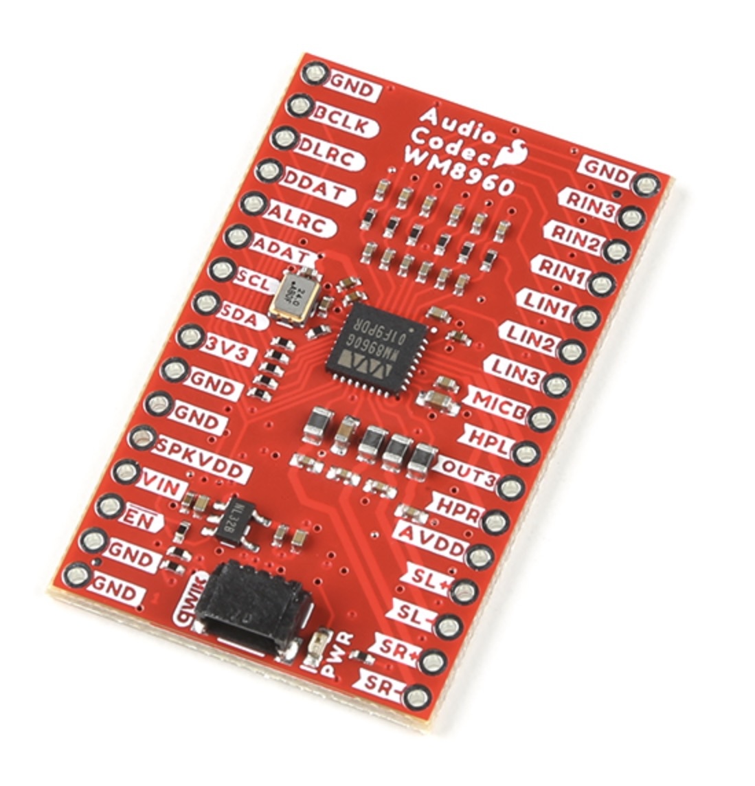
Again to get up and running as quickly as possible I looked for a chip with an existing breakout board and my research led to Sparkfun’s WM8960 breakout.
The huge plus is that Sparkfun has graciously blessed us with an Arduino library and extensive documentation, which proved invaluable to understand this chip.
Unfortunately this chip has reach the end of its product lifecycle and is now NRND, and none of the suggested replacement ICs have an affordable dev board.
The end goal being to create a custom PCB with all this, I will have to find a new codec.
Still a great choice as a learning tool.
MCU <> Codec Setup
By default the WM8960 is in its “off” state, it won’t power up any of its internals and won’t emit any sound.
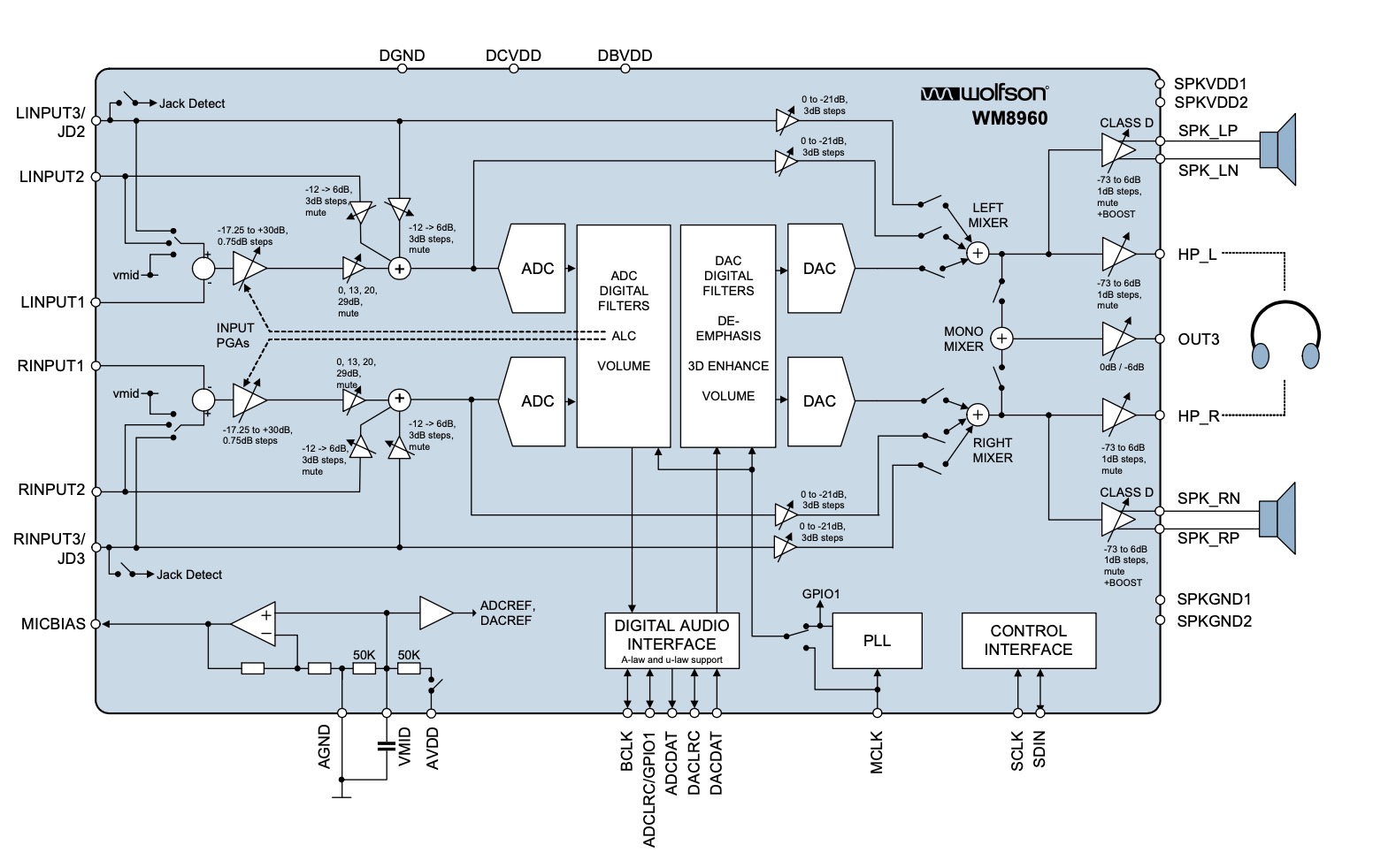
To configure it wee need I²C (Inter-Integrated Circuit), which is a nice and simple protocol that allows chips to talk to each other at relatively slow speeds, so it’s perfect for just setting up an IC.
I²C and the WM8960
MCU Configuration
We will need I²C to configure the codec, setting this up in CubeIDE is pretty simple.
These are my settings which are all the defaults. I’m using I2C1.
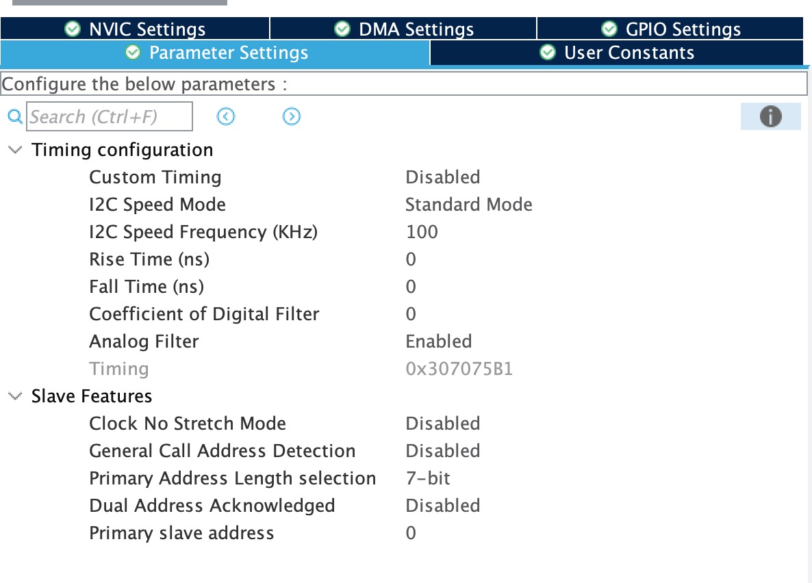
And these are the pins settings, also default.

WM8960 Configuration
I²C - Reading The Fantastic Manual
This proved particularly tricky and I spent a pretty huge amount of time trying to figure out what I had done wrong.
Well as it’s often the case, I hadn’t RTFM hard enough.
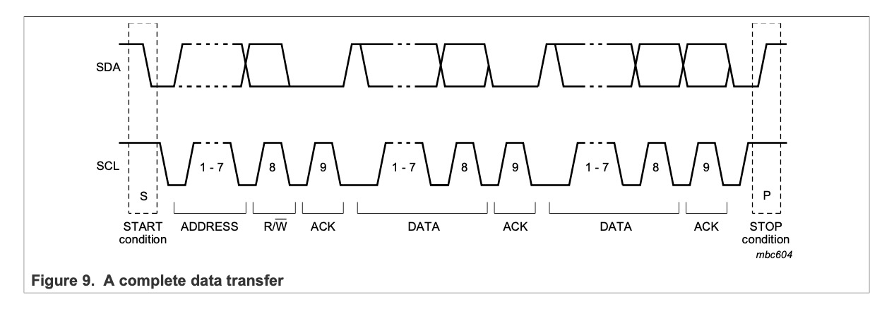
I had assumed that I²C communication is always following this data structure (from the master’s perspective, thus I’ll be ignoring the ACKs from the slave):
- Master writes the 7 bit address of the slave it wishes to address
- The 8th bit is the Read/Write bit
- Master writes the 8 bit register address it whishes to write to
- Master writes another 8 bit of data to be saved to that register
But I assumed wrong, the wikipedia article tells us:
Pure I2C systems support arbitrary message structures.
The only thing the specification stipulates, is that an ACK should be sent every 8 bits.
Here is an excerpt from the the datasheet(page 63):
The WM8960 is controlled by writing to registers through a 2-wire serial control interface. A control word consists of 16 bits. The first 7 bits (B15 to B9) are address bits that select which control register is accessed. The remaining 9 bits (B8 to B0) are data bits, corresponding to the 9 bits in each control register.

In case that wasn’t clear (wasn’t for me at first), all the register addresses in the WM89600 are actually only 7 bits, the 8th bit should be the Most Significant Bit (MSB) of the data you wish to write, which is 9 bits long (instead of the typical 8).
This makes is really hard to debug using a logic analyzer because the data that will be interpreted by your logic analyzer software will not make much sense when trying to compare it with the datasheet.
For instance, if you want to write 0x008 to the register 0x29.
You need to left shift by one the register address and jam your data’s MSB in
its place: (0x29 << 1) | (0x008 >> 8); and the of course omit your the MSB you
just added to the address from your data… (casting from uint_16 to uint_8 and
bit masking does the trick).

Which is very confusing because the register you wanted to address (say 0x29 for example) is
now left shifted once (so 0x58)… And your data also won’t look like what you
expect because it will be missing it’s MSB…
It’s messy, and I don’t think it’s very common… But that’s how this codec works.
Clock settings
I had a weird issue at first where after a random amount of time, the sound would sharply degrade
over the course of a few seconds all the way down to just noise.
Took me a while to figure out, in the end the issue turned out to be clock
related, my guess is that since the configuration was inacurrate, after some
time a desync would occur preventing proper function.
There are a few different clocks used in the codec, the main ones which are driving pretty much everything else are SYSCLK and MCLK.
On the Sparkfun board, MCLK cannot be changed as it’s provided by the 24MHz crystal oscillator soldered on the board and connected to pin 11 of the codec chip.
SYSCLK can be provided externally or derived from MCLK, the latter is what we’ll be using.
We also want a 48KHz sample rate, the datasheet tells us that we need a SYSCLK of 12.288 MHz.
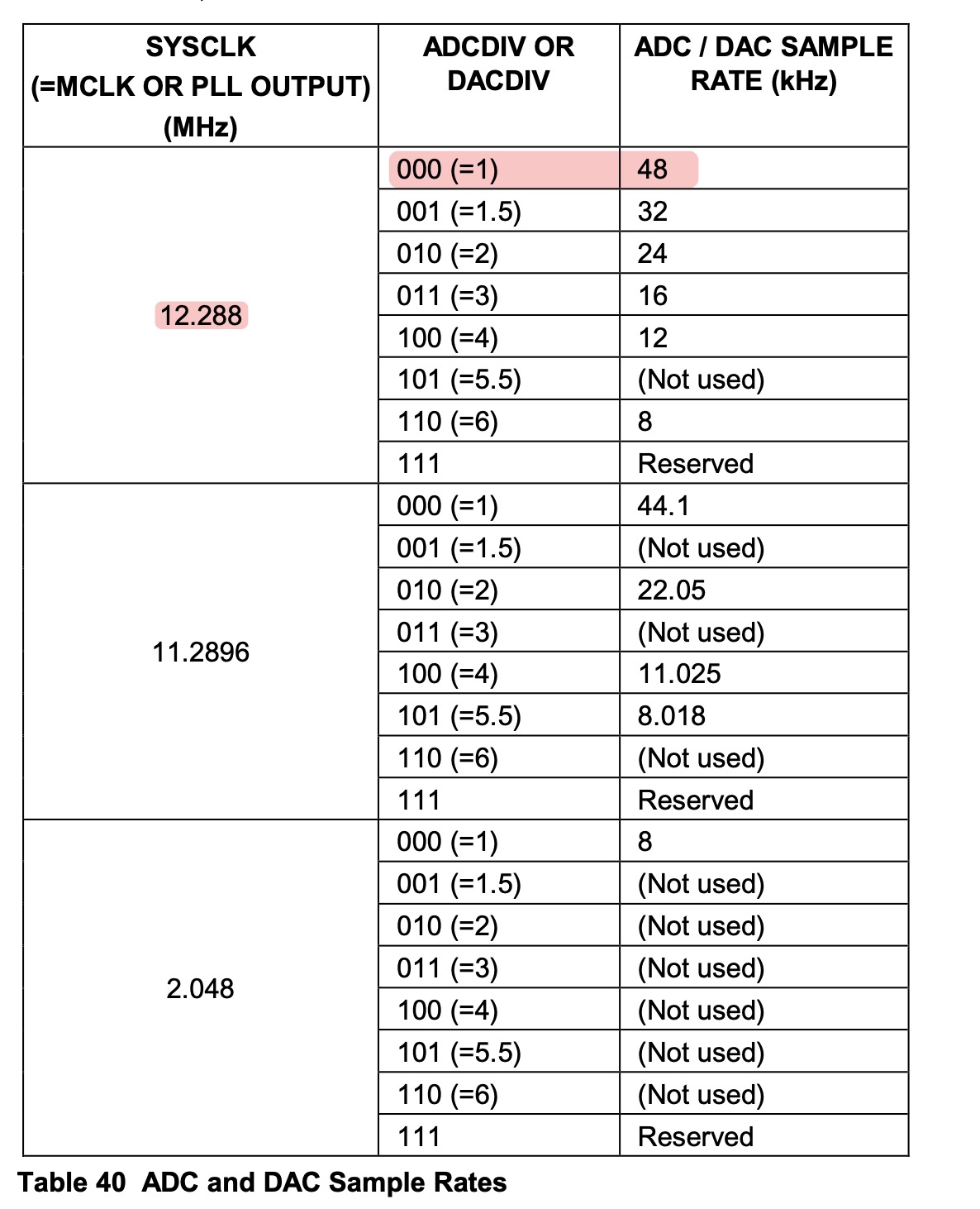
SYSCLK can be generated by a Phased-Locked Loop, (aka PLL) that uses MCLK as its input, the following table gives us the values we need to use:
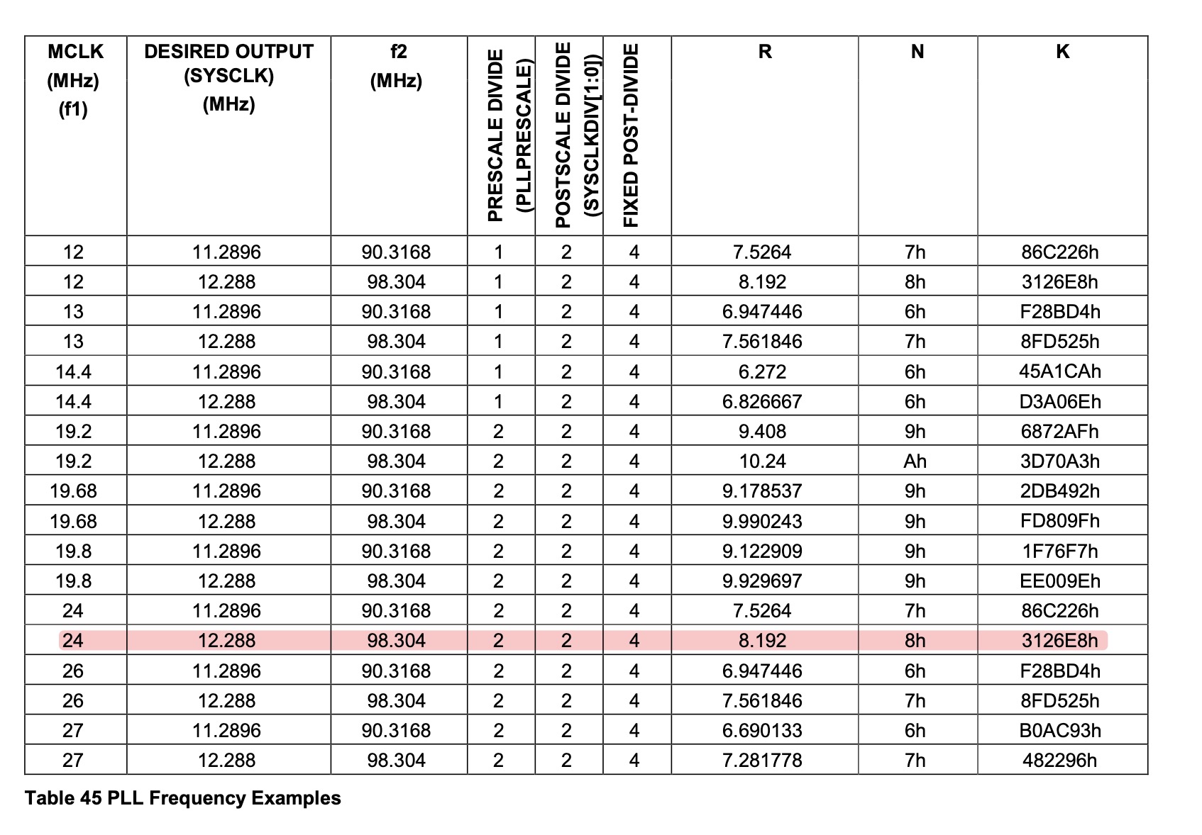
And this is achieved via the following snippet (full code available later in this article).
More information on these registers and values can be found on pages 59 and 60 of the datasheet for the codec.
...
  ret += _writeRegister(hi2c, 0x34, 0b000111000);
  ret += _writeRegister(hi2c, 0x35, 0x31);
  ret += _writeRegister(hi2c, 0x36, 0x26);
  ret += _writeRegister(hi2c, 0x37, 0xe8);
...
Code
In this configuration the Codec will only route the input audio from R/LINPUT2 to the ADC and then out the DAC to the headphone output.
The DAC and ADC word select lines are shared via the DLRC pin, do not use the ALRC pin as it’s configured as an output GPIO.
There may be some other things I’m missing… In any case this code can help but will likely not spare you a full read of the datasheet.
I’ve uploaded the full code in a public gist.
It’s also available under this collapsed section 👇
/*
 * wm8960.c
 *
 * Date: 2024-09-03
 * Author: @pyrho
 */

#include "wm8960.h"
#include "stm32h7xx_hal_def.h"
#include "stm32h7xx_hal_i2c.h"

static HAL_StatusTypeDef _writeRegister(I2C_HandleTypeDef *hi2c,
                                        uint8_t address, uint16_t data);
// P.63 of datasheet
// 7bit addr + R/W bit, MSB first
// The 7bit address is `0b0011010` the 8th bit is the R/W bit which needs to
// be set to `0` to be able to write.
// So this translates to 0x34 as stated in the datasheet
// Sparkfun uses `0x1A`, because they're using Arduino's "Wire" which I guess
// does the left shift on its own.
#define WM8960_I2C_ADDR 0x34

// Private API {{{
//

static HAL_StatusTypeDef _writeRegister(I2C_HandleTypeDef *hi2c,
                                        uint8_t address, uint16_t data) {

  // Shift the register address left 1 bit to leave room to the 9th
  // bit of the data
  uint16_t address_byte = address << 1;

  // Add the MSbit of the data to write to the register's address
  address_byte |= (data >> 8);

  uint8_t data_without_9th_bit = (0x00FF & data);

  return HAL_I2C_Mem_Write(hi2c, WM8960_I2C_ADDR, address_byte,
                           I2C_MEMADD_SIZE_8BIT, &data_without_9th_bit, 1,
                           HAL_MAX_DELAY);
}

// }}}

// Public API {{{

bool WM8960_isReady(I2C_HandleTypeDef *hi2c) {
  return HAL_I2C_IsDeviceReady(hi2c, WM8960_I2C_ADDR, 5, 100) == HAL_OK;
}

HAL_StatusTypeDef WM8960_init(I2C_HandleTypeDef *hi2c) {
  /*
   * #Observations
   * This these clock settings, this gives a SYSCLK @ 12.285MHz (close to the
   * reference 12.288)
   */
  HAL_StatusTypeDef ret = 0;

  // Reset
  ret += _writeRegister(hi2c, 0x0f, 0b000000001);

  // IPVU    > 8
  // LINMUTE > 7
  // LIZC    > 6
  // LINVOL  > 5:0
  // This is only for LINPUT1
  // ret += _writeRegister(hi2c, 0x00, 0b101111111);

  // PIVU    > 8
  // RINMUTE > 7
  // RIZC    > 6
  // RINVOL  > 5:0
  // This is only for RINPUT1
  // ret += _writeRegister(hi2c, 0x01, 0b101111111);

  // OUT1VU   > 8   > 1
  // LO1ZC    > 7   > 1
  // LOUT1VOL > 6:0 > 1111111 > = +6dB
  ret += _writeRegister(hi2c, 0x02, 0b111111111);
  ret += _writeRegister(hi2c, 0x02, 0b111111111);

  // OUT1VU   > 8   > 1
  // RO1ZC    > 7   > 1
  // ROUT1VOL > 6:0 > 111111 > = +6dB
  ret += _writeRegister(hi2c, 0x03, 0b111111111);
  ret += _writeRegister(hi2c, 0x03, 0b111111111);

  // Clocks {{{
  // ADCDIV    > 8:6 > 000
  // DACDIV    > 5:3 > 000
  // SYSCLKDIV > 2:1 > 10
  // CLKSEL    > 0   > 1
  ret += _writeRegister(hi2c, 0x04, 0b000000101);

  // OPCLKDIV    > 8:6 > 000  > don't care
  // SDM         > 5   > 1    > Fractional mode, because we need to provide the
  // factional part "K" of the PLL PLLPRESCALE > 4   > 1    > /2, see table P.
  // 61, values for 24MHz PLLN        > 3:0 > 1000 > 8, see table P. 61, values
  // for 24MHz
  ret += _writeRegister(hi2c, 0x34, 0b000111000);

  // 0x3126E8 => 0b 0011 0001 0110 1110 1000
  // 0x3126E8 => 0b 000011 00010110 11101000
  // input 24
  // desired: 12.288
  // prescale 2
  // sysclkdiv 2
  // R: 8.192
  // N: 0x8
  // K: 0x3126E8
  //
  // RES > 8 > 0
  // PLLK > 7:0 >
  ret += _writeRegister(hi2c, 0x35, 0x31);

  // RES > 8 > 0
  // PLLK > 7:0 >
  ret += _writeRegister(hi2c, 0x36, 0x26);

  // RES > 8 > 0
  // PLLK > 7:0 >
  ret += _writeRegister(hi2c, 0x37, 0xe8);

  // RES      > 8:7 > 00
  // ALRCGPIO > 6   > 1  > For debugging the clock
  // WL8      > 5   > 0
  // DACCOMP  > 4:3 > 00
  // ADCCOMP  > 2:1 > 00
  // LOOPBACK > 0   > 0
  ret += _writeRegister(hi2c, 0x09, 0b001000000);

  // }}}

  // Default clock is fine (but maybe not, since the datasheet only mentions a
  // max MCLK frequency of 12.288MHz, but the onboard xtal is 25MHz) According
  // to P.61 this is it. But actually if I want 48Khz, targeting 12.288 is
  // better that 11.2896 So for a 24Mhz crystal, this is better:
  // 24 12.288 98.304 2 2 4 8.192 8h 0x3126E8
  //

  // RES     > 8   > 0
  // DACDIV2 > 7   > 0
  // ADCPOL  > 6:5 > 00
  // RES     > 4   > 0
  // DACMU   > 3   > 0
  // DEEMPH  > 2:1 > 00
  ret += _writeRegister(hi2c, 0x05, 0b000000000);

  // DACVU   > 8   > 1
  // LDACVOL > 7:0 > 1111 1111 > 0dB
  ret += _writeRegister(hi2c, 0x0a, 0b111111111);
  // Doubled for VU
  ret += _writeRegister(hi2c, 0x0a, 0b111111111);

  // DACVU   > 8   > 1
  // RDACVOL > 7:0 > 1111 1111 > 0dB
  ret += _writeRegister(hi2c, 0x0b, 0b111111111);
  // Doubled for VU
  ret += _writeRegister(hi2c, 0x0b, 0b111111111);

  // RES  > 8   > 0
  // NGTH > 7:3 > 00000
  // RES  > 2:1 > 00
  // NGAT > 0   > 0     > Noise gate
  ret += _writeRegister(hi2c, 0x14, 0b00000001);

  // ADCVU   > 8   > 1
  // LADCVOL > 7:0 > 1111 1111 > 0000 0000 = 0db / 1111 1111 = +30dB / 0.5 steps
  // 0b11000011 = 0dB
  ret += _writeRegister(hi2c, 0x15, 0b111000011);
  // Doubled for VU
  ret += _writeRegister(hi2c, 0x15, 0b111000011);

  // ADCVU   > 8   > 1
  // RADCVOL > 7:0 > 1111 1111 > 0000 0000 = 0db / 1111 1111 = +30dB / 0.5 steps
  // 0b11000011 = 0dB
  ret += _writeRegister(hi2c, 0x16, 0b111000011);
  // Doubled for VU
  ret += _writeRegister(hi2c, 0x16, 0b111000011);

  // VMIDSEL > 8:7 > 01
  // VREF    > 6   > 1
  // AINL    > 5   > 1
  // AINR    > 4   > 1
  // ADCL    > 3   > 1
  // ADCR    > 2   > 1
  // MICB    > 1   > 0
  // DIGENB  > 0   > 0
  ret += _writeRegister(hi2c, 0x19, 0b011111100);

  // DACL   > 8 > 1
  // DACR   > 7 > 1
  // LOUT1  > 6 > 1
  // ROUT1  > 5 > 1
  // SPKL   > 4 > 1
  // SPKR   > 3 > 1
  // RES    > 2 > 0
  // OUT3   > 1 > 1
  // PLL_EN > 0 > 1
  ret += _writeRegister(hi2c, 0x1a, 0b111111011);

  // LMN1      > 8   > 0
  // LMP3      > 7   > 0
  // LMP2      > 6   > 0
  // LMICBOOST > 5:4 > 00
  // LMIC2B    > 3   > 0
  // RES       > 2:0 > 000
  ret += _writeRegister(hi2c, 0x20, 0b000000000);

  // RMN1      > 8   > 0
  // RMP3      > 7   > 0
  // RMP2      > 6   > 0
  // RMICBOOST > 5:4 > 00
  // RMIC2B    > 3   > 0
  // RES       > 2:0 > 000
  ret += _writeRegister(hi2c, 0x21, 0b000000000);

  // LD2LO    > 8   > 1
  // LI2LO    > 7   > 0
  // LI2LOVOL > 6:4 > 000
  // RES      > 3:0 > 0000
  ret += _writeRegister(hi2c, 0x22, 0b100000000);

  // RD2LO    > 8   > 1
  // RI2LO    > 7   > 0
  // RI2LOVOL > 6:4 > 000
  // RES      > 3:0 > 0000
  ret += _writeRegister(hi2c, 0x25, 0b100000000);

  // RES       > 8:7 > 00
  // LIN3BOOST > 6:4 > 000
  // LIN2BOOST > 3:1 > 100 > 000 = mute / 001 = -12dB / 111 = +6dB (3dB steps)
  // RES       > 0   > 0
  ret += _writeRegister(hi2c, 0x2B, 0b000001000);

  // RES       > 8:7 > 00
  // RIN3BOOST > 6:4 > 000
  // RIN2BOOST > 3:1 > 100 > 000 = mute / 001 = -12dB / 111 = +6dB (3dB steps)
  // RES       > 0   > 0
  ret += _writeRegister(hi2c, 0x2C, 0b000001000);

  // RES   > 8:6 > 000
  // LMIC  > 5   > 0
  // RMIC  > 4   > 0
  // LOMIX > 3   > 1
  // ROMIX > 2   > 1
  // RES   > 1:0 > 00
  ret += _writeRegister(hi2c, 0x2f, 0b000001100);

  // RES     > 8   > 0
  // GPIOPOL > 7   > 0
  // GPIOSEL > 6:4 > 100 > SYSCLK OUT
  // HPSEL   > 3:2 > 11
  // TSENSEN > 1   > 1
  // MBSEL   > 0   > 0
  ret += _writeRegister(hi2c, 0x30, 0b001001110);

  return ret;
}

// }}}
Inter-Integrated Circuit Sound (I²S)
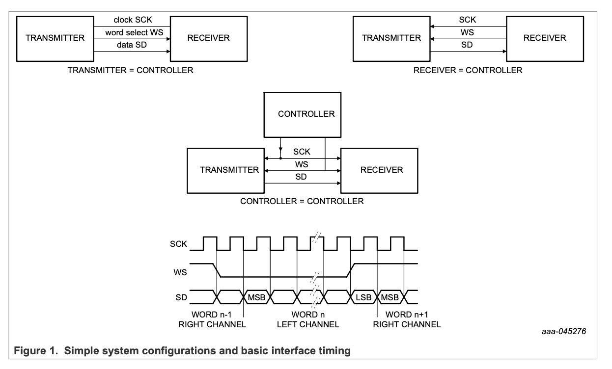
I²S is a protocol specifically designed to allow chips to exchange audio data.
It’s a 3-wire protocol:
- SD: The stream of audio bits
- WS: Left/Right channel selection, this is the sampling frequency
- CK: The Bit clock
The sample rate is determined by the frequency of the WS signal. At 48KHz/24bits stereo we have 48000 samples per seconds for two channels, and each channel contains 24 bits of data.

MCU Configuration
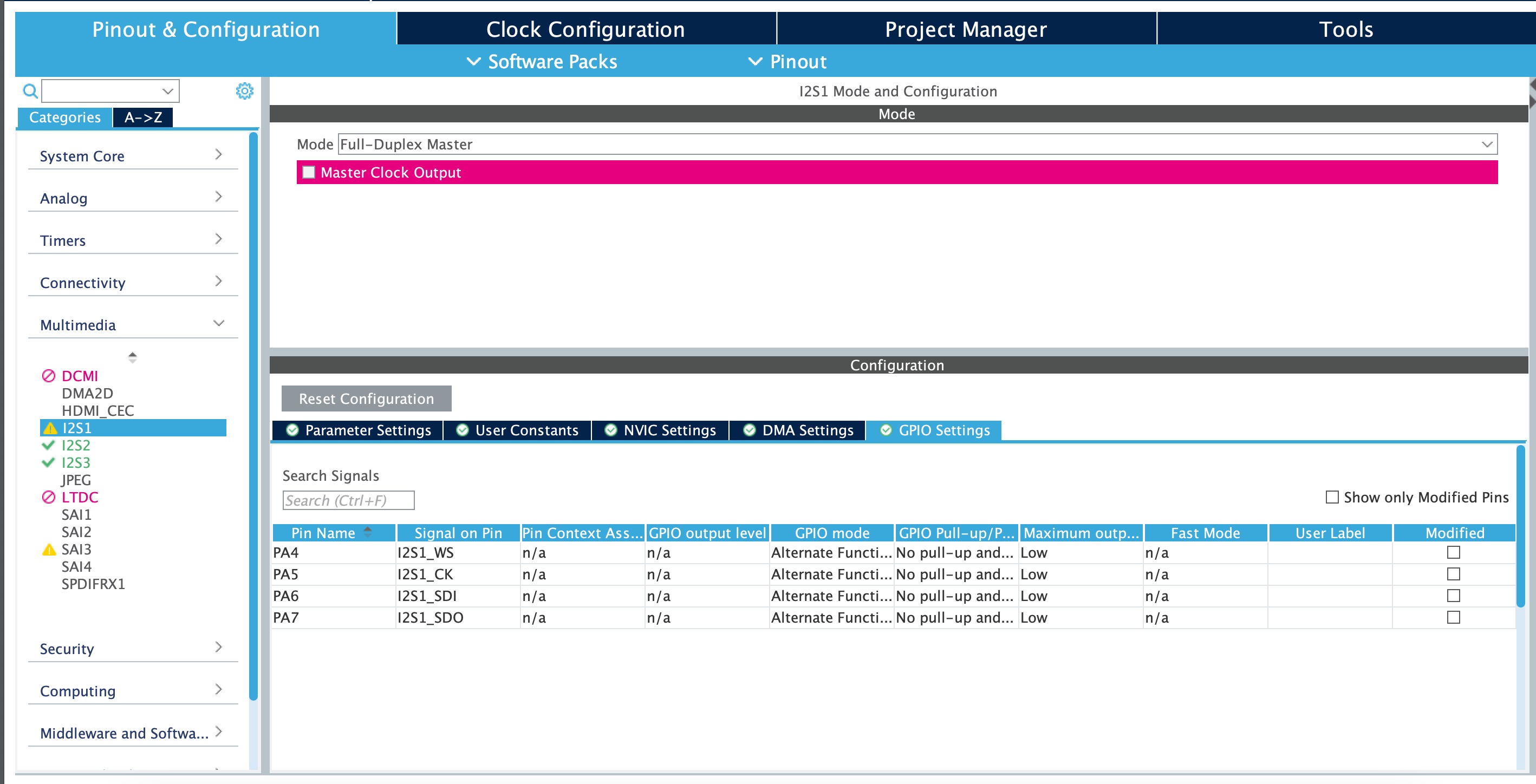
The STM32 will be communicating via I2S Full Duplex and act as the master. One “simplex” is used to receive data from the ADC, the other to send data to the DAC.
In full duplex there’s an extra “SD” wire to account for the extra communication channel.
Direct Memory Access (DMA)
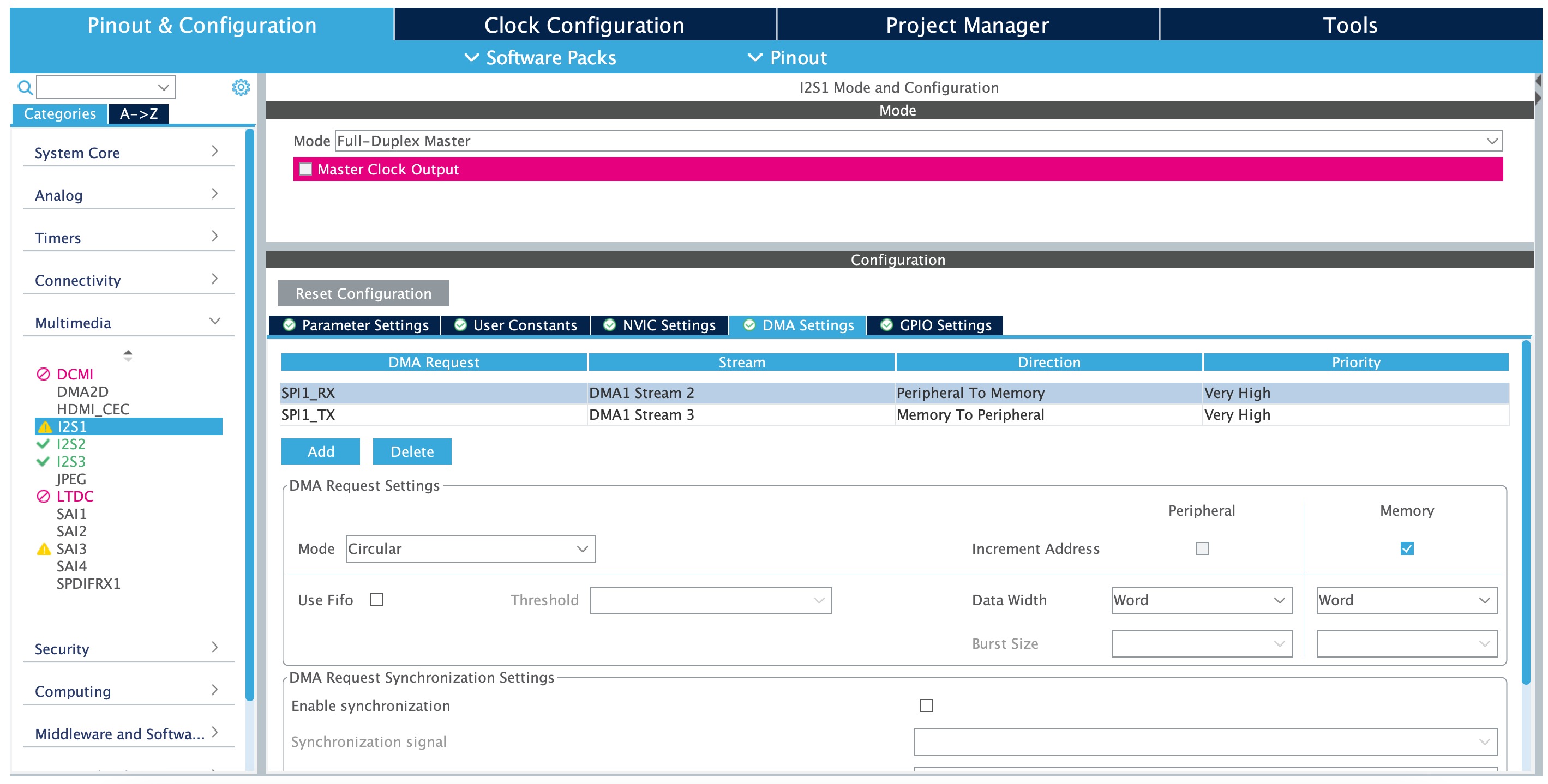
In order to process the audio in real time, your MCU can’t be polling the ADC to get its data or the audio will be choppy and of poor quality.
This is where DMA comes into play, DMA allows peripherals to access the memory directly bypassing the MCU’s main program.
In our case we’ll setup DMA so that the ADC can write to a circular buffer (circular means the buffer is of fixed size and the ADC will write over previous data in a circular fashion).
DMA also works by providing us with two callbacks, when the buffer is half
written and when it’s fully written.
This allows for what’s called a “ping pong” buffer, where we can process the
first half of the buffer while the ADC is writing the second half, and so on.
Please checkout Phil’s amazing video for more details on this topic.
Closing Notes
While this setup works and sounds can be heard clearly, I think there might still be an issue somewhere in my setup as the quality of my output signal when viewed on an oscilloscope is very poor and looks like noise; whereas it looks fine when bypassing my setup entirely (so it’s not a measurement issue… I think).
This is a raw-ish dump of my work on this so far so that I can refer to it in the future and hopefully it may help others on this mattter; but keep in mind this is all very “alpha” and ymmv.
Thanks o/